
CoolSem brings chip cooling into the wafer stack
This week, we spotlight the winners of the G&A Award 2026. Today: CoolSem Technologies.
Published on July 7, 2026
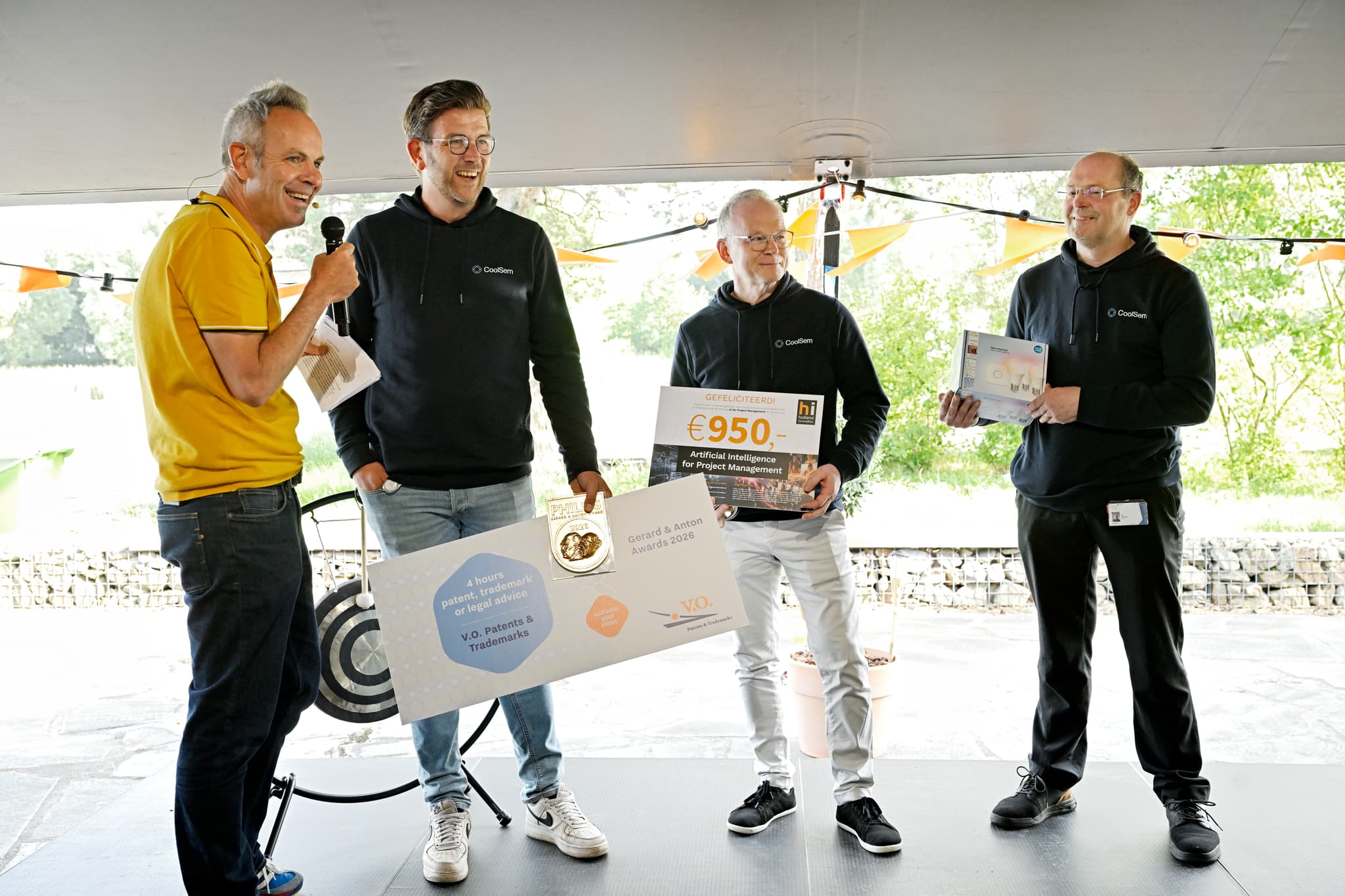
© Bart van Overbeeke Fotografie

Mauro swapped Sardinia for Eindhoven and has been an IO+ editor for 3 years. As a GREEN+ expert, he covers the energy transition with data-driven stories.
The semiconductor industry has a heat problem. As chips grow more powerful, they also run hotter. Higher temperatures reduce performance, shorten lifetime, and increase energy consumption. Conventional cooling solutions manage the heat after it has traveled through packaging layers. CoolSem Technologies is tackling the problem at the source.
"Today's chips generate increasing amounts of heat, while conventional packaging and substrate technologies struggle to remove that heat efficiently," explains CoolSem’s Chief Commercial Officer, Pieter Heersink. Their answer is WaLTIS® — Wafer-Level Thermal Integrated Substrate — a platform technology that creates a shorter and more efficient thermal path from the active device region to the cooling solution.
About CoolSem Technologies
A new thermal architecture
The core idea behind WaLTIS® is to remove the original semiconductor substrate — often one of the thermal bottlenecks in a device – and replace it with a precisely engineered multilayer thermal structure.
This replacement is optimized for heat transport, mechanical stability, and electrical performance. It brings thermal management into the wafer stack, rather than relying only on package-level cooling – such as liquid cooling solutions – after heat has already passed through thermally limiting layers.
A crucial design element is that the multilayered stack is engineered to meet the coefficient of thermal expansion (CTE) requirements of the device and its surrounding materials. CTE describes how much a material expands or contracts with changes in temperature. “Our design helps reduce thermo-mechanical stress and supports reliability during operation and thermal cycling. Depending on the application, device temperatures can be reduced by 25°C to 55°C or more,” underlines Heersink.
Ready for manufacturers
With a founding team having decades of experience in the semiconductor industry, CoolSem’s design has been ideated to fit existing manufacturing flows. The process is designed to be implemented at the wafer level, meaning that the innovative thermal stack can be applied to many devices in parallel, rather than chip by chip.
This choice gives WaLTIS® a path to scale without requiring device-to-device assembly or chip redesigns. For manufacturers, this is a crucial aspect: the best thermal solution is not very useful if it cannot survive the realities of semiconductor production.
From lab to industry
In its first year of operation, CoolSem has assembled a team, secured pre-seed funding from deep tech investors, and begun engaging with potential partners across the semiconductor and photonics ecosystem.
The company has moved past the initial laboratory proof-of-concept. The team is currently conducting a second technology validation run to demonstrate performance, repeatability, and manufacturability at the wafer level.
In parallel, CoolSem is in active discussions with companies in photonics, radiofrequency (RF) devices, power electronics, and other target markets to identify the strongest pilot opportunities. “Our goal is to demonstrate WaLTIS® on partner wafers or representative test vehicles where thermal performance is a critical bottleneck,” says Heersink.
Achieving this early validation will be key. The technology sits in a part of the semiconductor value chain where adoption decisions are highly evidence-driven. Companies considering a new semiconductor process need hard data before they commit engineering resources, qualification time, and capital.

G&A Awards 2026
Every year, we award 10 rising startups based in the Brainport region. In this series, you can get to know this year's winners better.
A valuable ecosystem to tap into
For a startup operating in the semiconductor industry, being in Brainport is a great advantage. “For an early-stage deep-tech company, this ecosystem is extremely valuable. Building a semiconductor-related company requires more than strong technology. It requires access to specialized knowledge, industrial partners, patient capital, and trusted networks that understand the long development and qualification cycles in this industry,” says the co-founder.
All of these elements can be found in Brainport. The support and the network of organizations such as PhotonDelta, Brabant Startup Fonds, and Brightmove have been instrumental in CoolSem’s first months. The presence of Eindhoven University of Technology has also been helpful, as was the access to the Rabobank Innovation Loan, which supported early technology development.
Global ambitions
The next phase calls for access to strategic industry partners, relevant pilot opportunities, and growth capital. “In short, we are looking for the right partners and resources to turn strong technical potential into industrial proof points,” underscores Heersink.
Should the pilots prove successful, CoolSem has even bigger ambitions, targeting advanced AI infrastructure and advanced computer systems. In these markets, thermal management is increasingly becoming a first-order design constraint.
If successful, CoolSem could turn chip cooling from a packaging afterthought into a core enabling technology for next-generation semiconductor and photonic devices. As AI and high-performance computing push hardware to its thermal limits, solving heat at the wafer level may become one of the industry's next decisive advantages.